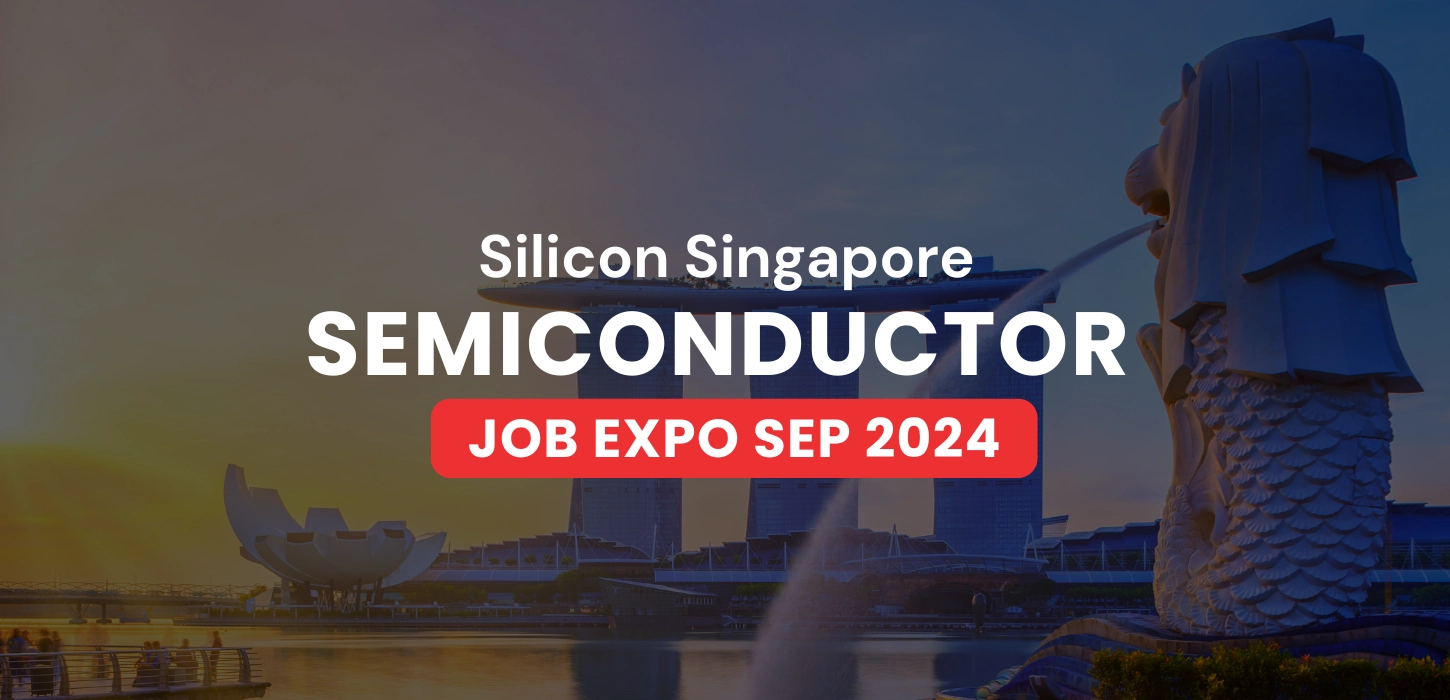
28 – 29 September 2024
9:30 am –
5:30 pm
Mercury III, Level 5, Furama RiverFront
405 Havelock Road, Singapore 169633
A diploma/bachelor’s in engineering.
Experience in preventive maintenance of semiconductor tools like Wet Etch, Dry Etch, Thin Film or Deposition tools.
Experience with associated equipment such as TEL furnaces, ASM tools, or final assembly and testing tools will be considered.
Ability to understand and work with electrical and mechanical schematics and diagrams and interpret operation manuals to perform preventive maintenance activities as per procedure.
Minimum 5 years of experience in semiconductor wafer FAB equipment maintenance is must.
In-depth knowledge of corrective & preventive maintenance of 200/300mm Wet Benches (SES, DNS, FSI Zeta) & Single wafer processing tools. (SEZ SP223/DVI, Semi tool spectrum, DNS, TEL, FSI).
Able to perform the robot teaching & adjustments for the above mentioned tools.
Responsible for Preventive and corrective maintenance of WET etch equipment’s.
Minimum 5 years of experience in global semiconductor wafer FAB equipment maintenance is essential.
Can Conduct corrective and preventive maintenance on Axcelis implanters NV-GSD-200E2, NV-GSD-HE & Varian EHP 500
Degree or Diploma in Engineering with relevant experience.
Minimum 6+ years of experience in Semiconductor metrology equipment maintenance.
Hands on experience is required for three or more of the following tools:
Hitachi SEMCD S9300, KLA-Tencor Archer 10 Overlay, KLA-Tencor HRP-220, Therma-wave Opti-probe, Rigaku-SYS3640, AMAT SEMvision200, KLA-Tencor SP1, KLA-Tencor defect inspection system, Rudolph Focus ellipsometer VIID.
Degree or Diploma in Engineering with relevant experience.
Work on cutting-edge projects in the world’s top semiconductor fabs, all while having the flexibility to thrive at home.
Orbit & Skyline is the best place to showcase your talent and experience. Embracing diverse cultures, it ensures your professional and personal growth. The supportive culture adds new dimensions to your development, enhancing decision-making skills. It’s truly the best family a workspace can offer!
ENGINEER
Joining Orbit & Skyline has been transformative. The environment fosters creativity, encourages innovation, and empowers employees to grow. From day one, I’ve been given the freedom to contribute to challenging projects. This company values individuality and nurtures talent, making it a beacon of excellence in the semiconductor industry. If you’re seeking a place where your skills are celebrated and your potential is unleashed, choose Orbit & Skyline.

ENGINEER
My seven-year tenure with Orbit & Skyline’s GFO team has been an extraordinary journey of professional growth and personal enrichment. Joining one of India’s pioneering semiconductor companies was an easy decision. The unique opportunity to travel globally, supporting tool installations and maintenance at various fabs, has been invaluable in honing my engineering skills and broadening my perspectives. This experience has been incredibly rewarding both professionally and personally.

ENGINEER
 Explore Orbit & Skyline Events
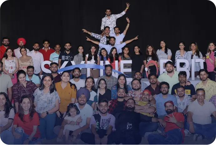 Explore Company Culture