Driven by Passion for Excellence

At Orbit & Skyline, we specialize in delivering cutting-edge engineering solutions for semiconductor manufacturing. With a focus on cost optimization, product development, and advanced simulations, we help businesses stay ahead in a rapidly evolving industry.
With a strong foundation in engineering innovation, we help semiconductor manufacturers reduce costs, enhance product reliability, and accelerate time-to-market. By leveraging advanced modeling, additive manufacturing, and obsolescence management, we provide customized solutions tailored to meet the industry's most demanding challenges.


At Orbit & Skyline, we specialize in delivering cutting-edge engineering solutions for semiconductor manufacturing.
View Case studies


At Orbit & Skyline, we specialize in delivering high-quality engineering solutions tailored to the evolving needs of the semiconductor and manufacturing industries. We have a strong foundation in semiconductor tool engineering, providing innovative solutions to meet the industry's most complex challenges.

Reduce costs while maintaining top-tier performance.

Trusted by top companies for cutting-edge, scalable solutions.

Predict, optimize, and improve designs with FEA, CFD, and FNM.

Comprehensive support from concept to delivery for optimal results.


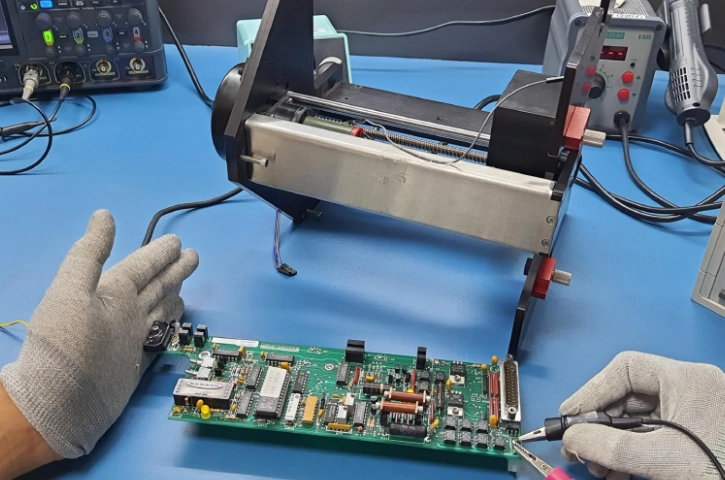
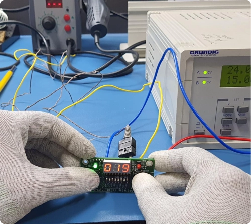
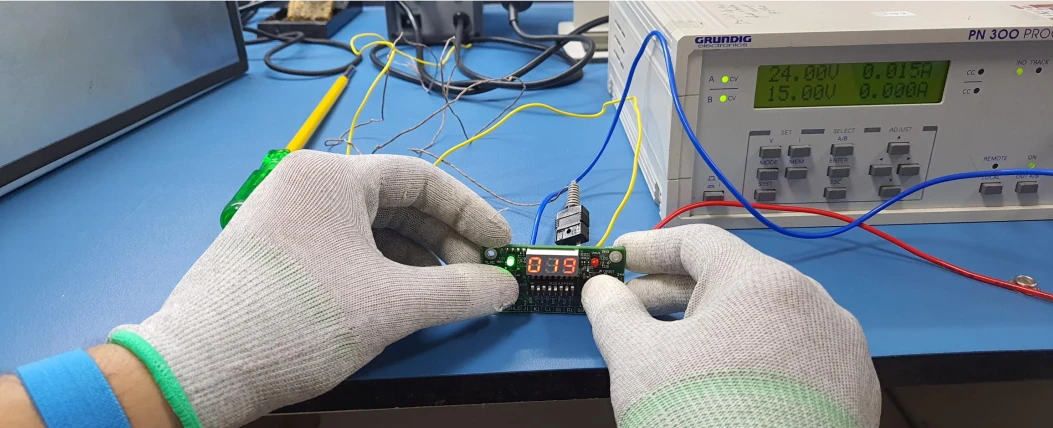
The objective was to design and develop a blackbox temperature limit controller to replace unreliable, locked-out supplier solutions. The controller needed to monitor critical temperature thresholds and execute safety interlocks in real time. The solution had to be plug-compatible, configurable, and long-term supportable—ensuring seamless integration into existing tool environments without depending on external OEM vendors.
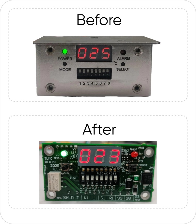
The primary objective was to develop a fully compatible form-fit-function replacement for the legacy controller, capable of supporting four distinct configurations. The replacement had to integrate seamlessly with the existing tool infrastructure while meeting all required functional, electrical, and regulatory compliance standards.

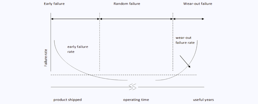
In the current era of rapid technological changes, the electronic industry is evolving at a lightning speed. The shorter life span of the components is posing a severe sustaining threat to equipment manufacturers, due to mismatch in the component and the equipment's’ lifecycle.
At Orbit & Skyline , through our excellent obsolescence management process and deep engineering capabilities, we provide a comprehensive sustaining solution to all type of obsolescence issues.
 End to end solutions to OB problems
 Qualification plans (in case replacement need field testing)
 Speed to solution at a low cost
 Deploy engineering resources on high value new product development
 Tested prototypes
 Installation procedures
 Extended product lifecycle
 Electronic Component Lifecycle (4-5 Years)

 Semiconductor Equipment Lifecycle (25-30 Years)
Electronic components last about 4–5 years due to rapid tech updates, while semiconductor manufacturing equipment is built to last 25–30 years and requires regular maintenance.
Overall responsibility of managing product lifecycle
 Risk ranking of BOM components
 Tailored strategy to address parts under different risk categories
 Alternate drop-in part recommendation
 Upgrade/retrofit kits, where no drop-in replacement available
 Reverse engineering
Repair/refurb
Reverse engineering
Repair/refurb
Orbit & Skyline has deep mechanical, electrical and electronics expertise in semiconductor industry to support multi disciplinary engineering programs at tool, module and sub module level.
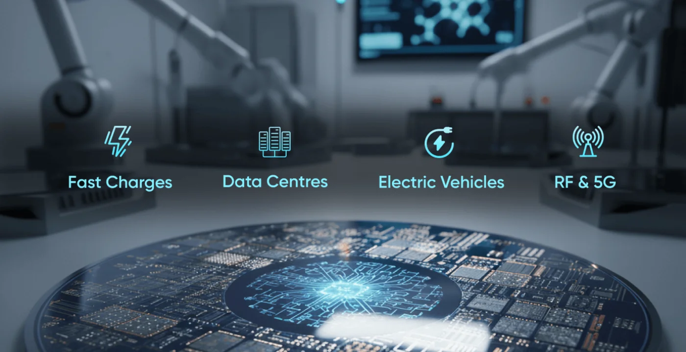
Our core competencies include gas boxes, RF engineering, PCB, local Power boxes, MPDs, design of process critical parts like pedestals, showerheads, ESCs.
Round-the-clock design support
Better efficiency, shorter design cycle, faster releases
Cost effective
Ownership of design
Manufacturing coordination
Product lifecycle management
Conceptual design

Orbit & Skyline helps you achieve your design goals faster and better. Our team of modeling experts work with you to understand the real boundary conditions for accurate results and flawless design solutions. We reduce the need for costly and time-consuming experimental testing by advanced modeling which also minimizes the risk of design failure and the number of design/prototyping iterations.
With advanced modeling and simulations, you can avail these key benefits:
 Lower design failure risk
 Fewer design and prototyping iterations
 Cost saving
 Faster design and development cycle
 Structural Analysis: Helps to determine the cause of structural failure. Highly beneficial while optimizing material, strength, cost, weight, etc.
 Computational Fluid Dynamics: Can determine pressure drop, flow path, flow rates, pattern etc. which is really helpful in design of gas distribution system, pipe/tube routing and nozzle/showerhead designs.
 Flow Network Modelling: Helps to understand the gas distribution and transmission systems and possible failure root causes.
 Thermal Analysis: Helps to study the properties of material with change in temperature.
 Multiphysics Analysis: Includes study of heat transfer, fluid flow, deformation, electromagnetics and mass transport.

In today’s technology driven world, it’s really important to adapt to the digital age as the ecosystem is transforming around it which is helpful for both engineering as well as suppliers in improving overall efficiency and ease.
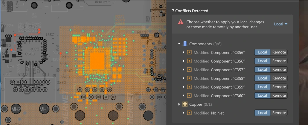
At Orbit & Skyline, we’ve got a team with rich experience in DT(Model Based Definition) which helps in establishing the MBD process which enable engineers to create, manage, and communicate product design information more efficiently and accurately.
 Faster product launch: Making CAD as a master streamline the Design and Development process
 Accurate cable/tubes length as we can model them and visualize the routing
 Reduction in documentation time due to CAD as master
 Easy visualization for field engineers
 Faster part Quality review (CAD based)
 Reduction in manual work, improved automation
 Complete ownership on pilot/testing and establishing the MBD process in the organization
 Supplier qualification support
 Conversion of existing parts into MBD parts
 Training and awareness to the engineers

In the fast-paced world of semiconductor manufacturing, cost efficiency is critical. The increasing complexity of fabrication equipment and the rising cost of raw materials pose significant challenges for manufacturers. Value Engineering (VE) is a structured approach that helps optimize costs while maintaining or improving performance and reliability.
At Skyline, through our expertise in value engineering and deep technical capabilities, we provide comprehensive solutions to optimize semiconductor equipment costs without compromising functionality.
 Systematic cost reduction without performance degradation
Standardization of components for cost efficiency
Systematic cost reduction without performance degradation
Standardization of components for cost efficiency
 Material and design optimization for durability
 Process improvements for enhanced operational efficiency
 Faster time-to-market with streamlined solutions
 Increased equipment lifespan and reliability
 Strategic resource allocation for innovation

 Comprehensive assessment of equipment design for cost-saving opportunities
 Function-based analysis to eliminate unnecessary expenses
Supplier collaboration to achieve volume discounts and material alternatives
Function-based analysis to eliminate unnecessary expenses
Supplier collaboration to achieve volume discounts and material alternatives
 Proactive risk management to prevent cost overruns
 Standardized and modular design implementation
 Substitution of high-cost materials with cost-effective alternatives
 Lifecycle cost analysis for long-term savings
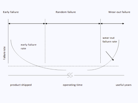
Orbit & Skyline is a leading Reliability service and solution provider in the semiconductor industry. We help our customers to track and maintain the performance of the Semiconductor equipment during the entire product development life cycle. Our expertise includes Design for Reliability, Reliability Test Planning, Failure Report Analysis and Corrective Action System (FRACAS) and Aftermarket Reliability services.
We are aligned with E10 standard to provide reliability-driven solutions to our customers in terms of product robustness, enhanced design margin and minimum field failures, which in turn reduce warranty costs. Partner with us to develop, maintain and integrate a robust semiconductor ecosystem to win customer support.
 Design for Reliability (DfR): Identify design margins, robustness, and potential failure modes.
 Reliability Goals: Set and allocate measurable reliability targets for each subsystem.
 Advanced Reliability Testing: Execute HALT, HASS, and other tests for durability validation.
 Forecasting: Use statistical tools like Weibull to model and predict failures.
RAMS Reports: Customer wise quarterly report.
Forecasting: Use statistical tools like Weibull to model and predict failures.
RAMS Reports: Customer wise quarterly report.
 Data-Driven Analysis: We use tools like Pareto, 8D, and Process FMEA for root cause analysis.
 FRACAS: Maintain a close loop system to identify, capture and address the design and process weak links.
 Warranty Analytics: Track annualized failure rates and estimate reserves for critical parts.
CIPs: Drive CIPs with respective functional groups to address systematic issues.
Warranty Analytics: Track annualized failure rates and estimate reserves for critical parts.
CIPs: Drive CIPs with respective functional groups to address systematic issues.
Spares product management involves overseeing the lifecycle of spare parts and components for semiconductor equipment or products. This service ensures that customers (e.g., manufacturers or end-users) have access to critical replacement parts to maintain operational continuity, minimize downtime, and extend the lifespan of semiconductor-based systems.
 Inventory Management: Maintain an optimized stock of spare parts like wafers, photomasks, or chip modules, balancing cost and availability.
Demand Forecasting: Predict customer needs based on equipment usage patterns and failure rates.
Inventory Management: Maintain an optimized stock of spare parts like wafers, photomasks, or chip modules, balancing cost and availability.
Demand Forecasting: Predict customer needs based on equipment usage patterns and failure rates.
 Supply Chain Coordination: Partner with suppliers to ensure timely production and delivery of spares.
 Customer Support: Provide technical guidance on spare installation and compatibility.
 AI: Predictive maintenance, demand forecasting, inventory optimization, risk mitigation, waste reduction.
 BI: KPI dashboards, root cause analysis, management cockpit views.
 Data Science: Inventory planning analytics, pattern recognition, scenario simulation.
 Zero Downtime: Fast access to critical parts keeps operations running.
 Extended Equipment Life: Timely replacements reduce wear and tear, boosting longevity.
 Smart Inventory, Lower Costs: Balanced stock avoids overbuying and shortages.
 Proactive Support: Forecasting and expert guidance prevent last-minute chaos.
 Stronger Supply Chain: Seamless coordination ensures spares are always on hand.
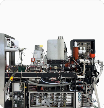
Equipment Engineering focuses on designing, optimizing, and supporting semiconductor tools. It includes wet clean optimization, field readiness, product support, and global field operations, ensuring efficient, high-quality, and continuous production.
 Wet Clean Optimization: Enhancing wet clean processes through tool standardization, localized instructions, data-driven insights, and expert engineering support.
 New Product Field Readiness: Ensuring successful product launch through market validation, strategic planning, cross-functional coordination, and comprehensive field readiness support.
 Global Product Support: Delivering global technical support through timely issue resolution, user guidance, knowledge sharing, and collaboration with development teams.
 Global Field Operations: Driving field team success globally through process optimization, data-driven insights, enablement support, and seamless cross-functional coordination.
 Less Downtime, More Uptime: Smart procedures, visual aids, and robotics-led support keep tools running longer and cleaner.
 Stronger Yields, Smarter Processes: Data-driven PM methods and custom hardware reduce variation, boost consistency, and improve process outcomes.
 Automation-Ready Maintenance: Robotics integration ensures seamless preventive care—designed to scale with advanced nodes and toolsets.
 Lower Cost of Ownership: Enhanced consumables life and efficient maintenance routines cut unnecessary costs and extend tool life.
 Expert-Led Support: A fusion of semiconductor veterans, robotics specialists, and technical content creators for comprehensive coverage.
 Tailored to Your Fab: Multilingual content, CAD-led customizations, and site-specific solutions for smooth implementation across geos.
Legacy Product Ownership involves the ongoing management, support, and optimization of older semiconductor products, components, or equipment that remain critical to customers or internal operations. For a semiconductor services manufacturer, this service ensures that legacy chips, modules, or fabrication tools—often from previous generations (e.g., 28nm, 45nm nodes)—continue to meet performance, reliability, and supply demands. It bridges the gap between obsolescence and the needs of industries like automotive, industrial, or aerospace, where long product lifecycles are common.
Product Lifecycle Extension: Maintain production, redesign components, and qualify alternatives to extend the life of legacy products.
 Supply Chain & Obsolescence Management: Secure critical materials, manage EOL parts, and plan proactive obsolescence strategies.
 Technical Support & Maintenance: Provide repairs, detailed documentation, and remote/on-site assistance for legacy systems.
 Software, Firmware & Compatibility Updates: Patch outdated systems, ensure compatibility with modern environments, and develop bridging solutions.
Reverse Engineering & Redesign: Recreate obsolete products using modern tools while preserving performance and specs.
Software, Firmware & Compatibility Updates: Patch outdated systems, ensure compatibility with modern environments, and develop bridging solutions.
Reverse Engineering & Redesign: Recreate obsolete products using modern tools while preserving performance and specs.
 Operational Continuity: Ensures critical legacy systems remain functional in industries with long lifecycles.
Cost Savings: Avoids the high cost of immediate upgrades by extending the life of existing assets.
Operational Continuity: Ensures critical legacy systems remain functional in industries with long lifecycles.
Cost Savings: Avoids the high cost of immediate upgrades by extending the life of existing assets.
 Risk Mitigation: Minimizes disruptions through proactive planning and reliable support.
 Customer Confidence: Builds trust with long-term support and stability for essential systems.
 Seamless Transition Paths: Enables smooth migration to newer technologies with minimal disruption.
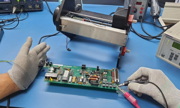
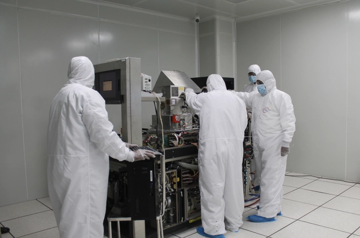
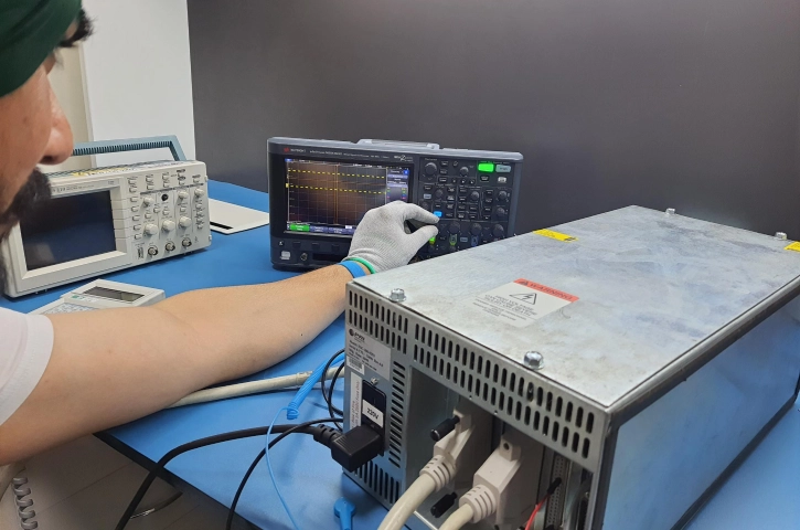
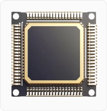
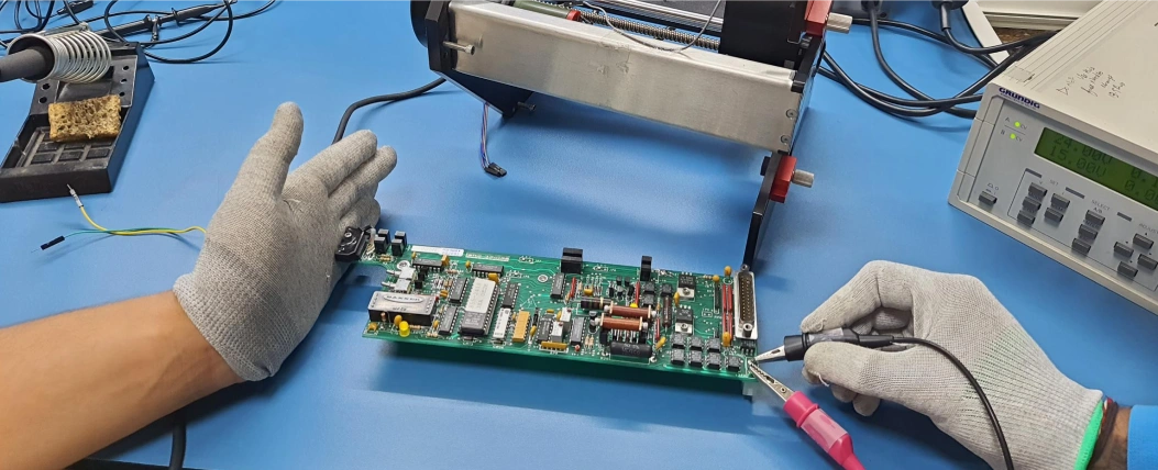
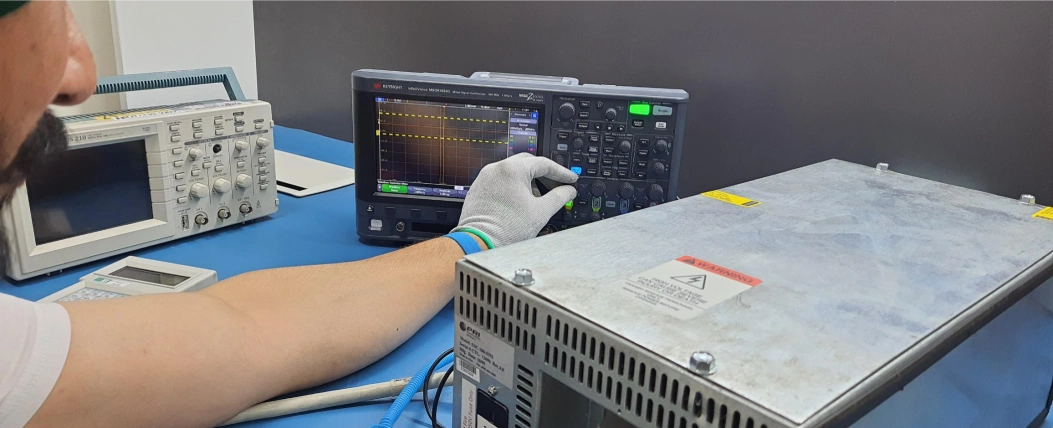
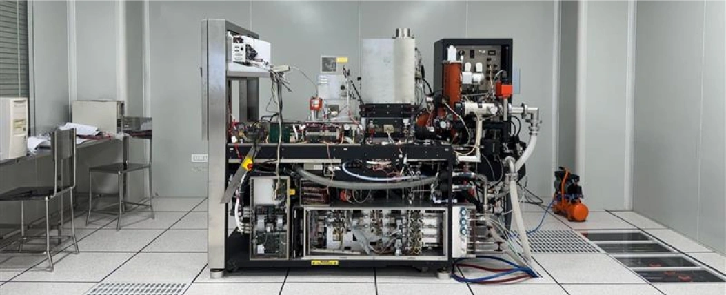
Hardware Engineering in semiconductor services involves the design, development, testing, and optimization of physical electronic systems built around semiconductor components. This includes everything from board-level hardware, high-speed PCB design, and system validation to component lifecycle management and compliance. These services ensure that semiconductor-based products are reliable, manufacturable, and ready for real-world deployment across industries such as automotive, industrial automation, aerospace, and telecom. The goal is to bridge innovation with practicality—delivering hardware solutions that are not only high-performing but also scalable, cost-effective, and future-proof.
 New Product Development: Designing and prototyping the hardware to detect and rectify flaws before full-scale production
 Upgrades/CIPs: Implementing continuous improvement projects and hardware upgrades to enhance tool performance and reliability.
 Centre of Excellence: Driving specialized hardware innovation through expertise in FEA (Finite Element Analysis), gas delivery systems, power design, additive manufacturing, RF, and PCB engineering.
 Accelerated Time-to-Market: Efficient design cycles and validation processes reduce product development timelines.
 Optimized Performance & Reliability: High-quality engineering ensures robust operation, even in high-stress or critical-use environments.
 Lifecycle Risk Reduction: Proactive component management avoids redesigns and obsolescence surprises.
 Cross-Industry Applicability: Supports diverse domains—automotive, industrial, telecom, aerospace—via customized hardware platforms.

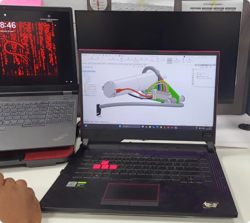
Additive Manufacturing (AM), commonly known as 3D printing, is revolutionizing semiconductor hardware and tooling development by enabling rapid, precise, and cost-effective production. In a semiconductor services environment, AM is used to create prototypes, custom fixtures, tooling, and low-volume parts with high precision. This approach allows for accelerated product development, reduced dependency on traditional supply chains, and greater design flexibility—especially beneficial in cleanroom environments or high-performance packaging scenarios. By integrating AM into the semiconductor workflow, companies can innovate faster, respond to design changes on the fly, and optimize production without the constraints of conventional manufacturing methods.
 Rapid Prototyping for Components: Quickly produce functional prototypes of semiconductor fixtures, enclosures, and tooling for design validation.
 Low-Volume Custom Part Production: Create highly customized or low-quantity parts without the cost of traditional tooling or molds.
 Material Development & Testing: Experiment with high-performance materials (e.g., heat-resistant, conductive polymers) suitable for semiconductor environments.
 Design Optimization & Iteration: Use topology optimization and fast iteration cycles to reduce weight, improve strength, or enhance thermal management.
Faster Product Development: Reduces lead time from concept to part, accelerating R&D and innovation cycles.
Cost Efficiency for Customization: Eliminates tooling costs for small-batch or highly specific designs.
Greater Design Freedom: Enables complex geometries and integrated features that are hard to achieve with traditional manufacturing.
On-Demand Manufacturing: Supports just-in-time production, reducing inventory and waste.
Design Optimization & Iteration: Use topology optimization and fast iteration cycles to reduce weight, improve strength, or enhance thermal management.
Faster Product Development: Reduces lead time from concept to part, accelerating R&D and innovation cycles.
Cost Efficiency for Customization: Eliminates tooling costs for small-batch or highly specific designs.
Greater Design Freedom: Enables complex geometries and integrated features that are hard to achieve with traditional manufacturing.
On-Demand Manufacturing: Supports just-in-time production, reducing inventory and waste.