1
IP Transfer
Secure, efficient transfer of intellectual property, enhancing technological edge.

At Orbit & Skyline, our Process Engineering Team comprises experts with extensive experience in High Volume Manufacturing (HVM) at leading fabs such as Intel, Micron, and Global Foundries.
Our diverse team includes PhD holders and esteemed professors who excel in setting up advanced labs and guiding the next generation of engineers. We specialize in CMOS and Compound Semiconductor Fabs, offering comprehensive support from tool and process qualification to unit step, module development, and technology transfer.
We tailor our process engineering services to meet your fab's specific needs. Whether you're scaling, optimizing, or transitioning technologies, our solutions are built to fit.

Our team facilitates seamless technology transfer between fabs, manages integration challenges, optimizes processes, and sustains high-quality output across multiple facilities.

We ensure production-ready tools and processes support qualification, optimization, and integration to achieve reliable and efficient fab operations.
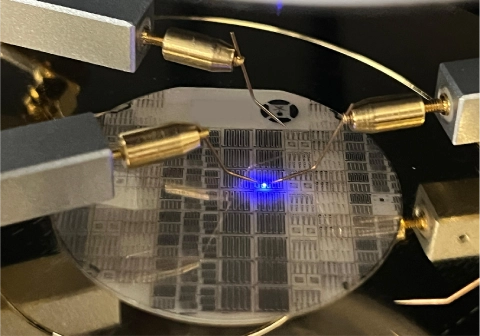
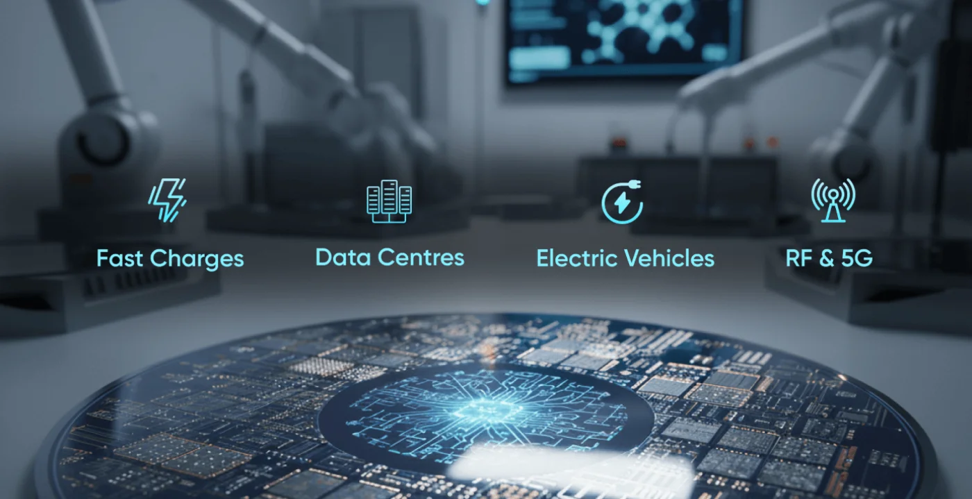
We specialize in compound semiconductor fabs, guiding epitaxial growth and process development for GaN, GaAs, and other materials using MOCVD and MBE technologies.

From specification finalization and mask design to fabrication and packaging, we provide comprehensive support for developing high-power electronics, optoelectronics, and MEMS devices.
Our well-regarded Process Engineering Team comprises global specialists with experience from leading fabs such as Intel, Micron, and GlobalFoundries, as well as with OEMs like AMAT and LAM, has been delivering reliable solutions across the semiconductor Industry. With expertise spanning CMOS and compound semiconductors, we offer unparalleled support in process development, technology transfer, and workforce training, ensuring your success.

Strong partnerships with OEMs like AMAT and LAM, and with Fabs such as Intel, Micron, and GlobalFoundries.

Advanced Lab Setup and Workforce Training

Specialization In CMOS and Compound Semiconductors

Global Perspective with Local Agility

End-To-End Process Engineering Support

Seamless Technology Transfer and Integration
IP Transfer
Secure, efficient transfer of intellectual property, enhancing technological edge.
Device Integration
Seamless integration of devices into production for smooth operations.
Line Sustaining
Continuous monitoring to maintain and optimize production line performance.
Yield Improvement
Implementing strategies to maximize yield and boost production output.

Custom processes for optimal manufacturing.

Smooth integration and operation across fabs.

Expertise in GaN and GaAs materials using MOCVD and MBE.

Identifying and addressing production gaps for seamless operation.

In production fabs, newly installed or upgraded tools often face long delays before they contribute to real product output. In this case, the goal was to:
To overcome these timeline bottlenecks, a dual-track strategy was adopted—advancing tool and process qualification on one track while building the product enablement infrastructure in parallel. Both paths converged at a single point, enabling the tool to become production-ready immediately upon acceptance.
We provide end-to-end process engineering solutions, including process flow development, tool and process qualification, technology transfer, yield enhancement, and comprehensive workforce training. Whether for CMOS or compound semiconductor fabs, our services are tailored to your specific production needs.
We do both. Whether you're establishing a new fab, expanding capacity, or optimizing existing lines, our end-to-end process engineering services from tool qualification to technology transfer are tailored to your unique goals.
Simply reach out via our contact page. We'll discuss your fab's specific goals and challenges, then create a customized roadmap, whether you need faster tool ramp-up, seamless technology transfer, or optimized compound semiconductor processes.
Yes. We specialize in compound semiconductor manufacturing, guiding epitaxial growth using MOCVD and MBE technologies for GaN, GaAs, and related materials. We also support full device development for high-power and optoelectronic applications.
Absolutely. Our team includes PhDs, industry veterans, and former professors who excel at establishing advanced labs and delivering comprehensive hands-on training to upskill your engineers and operators.