Your Partner in Custom Semiconductor Design Services

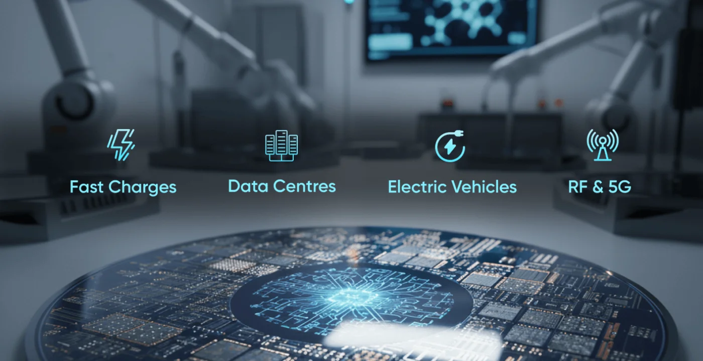
We specialize in delivering VLSI design services tailored to meet diverse customer needs. Our team is proficient in advanced IC design methodologies, foundry and PDK selection, comprehensive VLSI design flows, and managing tape-out processes.
We excel in working with industry-standard EDA tools from leading vendors and can seamlessly integrate mixed-tool flows based on customer-specific requirements and license availability. This adaptability enables us to support our clients in achieving their goals by leveraging our expertise in diverse design flow capabilities.
Our services cater to government entities, private sector organizations, and academic institutions. By utilizing our innovative design workflows, we simplify the IC design process, making it more accessible and cost-effective. With a proven history of successful tape-outs and end-to-end support, Orbit & Skyline is your trusted partner in advancing semiconductor innovation.

Define Specification, schematic design,
SPICE simulation
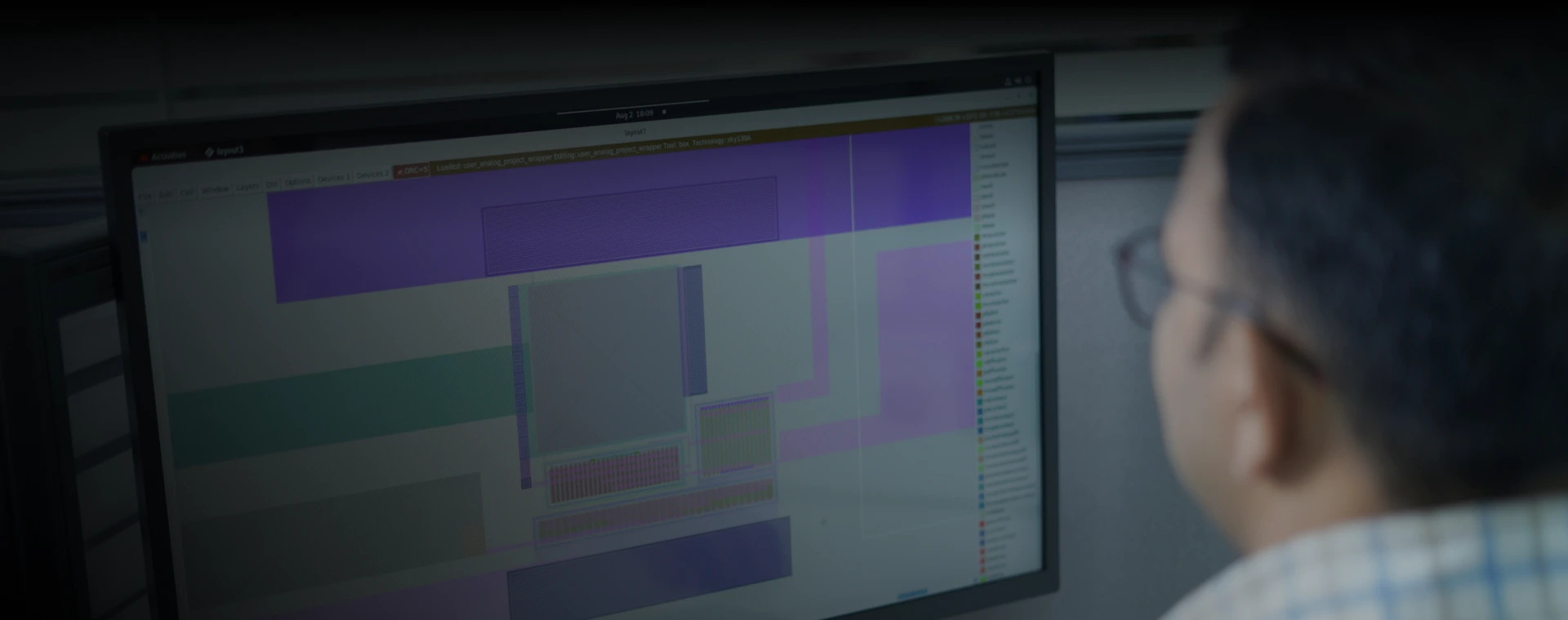
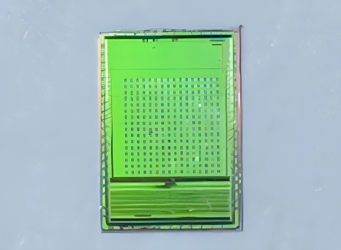
Custom IC layout, placement, routing
DRC, LVS, and PEX verification
Chip finishing, meeting foundry
requirements, and facilitating foundry
interactions

 Step 1
 Step 2
 Step 3
 Step 4

We specialize in semiconductor design services, providing tailored solutions to meet diverse customer requirements. With expertise spanning advanced IC design methodologies, foundry and PDK selection, and seamless tape-out management, our team ensures reliable and innovative design outcomes.

Comprehensive Expertise Across Design Spectrum

Adaptable and Scalable Design Workflows

Focus on Accessibility and Cost-Effectiveness

Commitment to Collaboration and Support Bottom of Form
Orbit & Skyline has made significant investments in supporting legacy tool management. The cornerstone of this investment is the Orbit & Skyline Center of Excellence, a state-of-the-art facility designed specifically to tackle the unique challenges of legacy tools.
15,000 ft2 total floor area

1,500 ft2 class 10k cleanroom (expandable to 3,000 ft2)

1,400 ft2 manufacturing & storage area

600 ft2 training lab with advanced pneumatic, servo, and PLC systems

One of our international clients approached us with a specific requirement: to train their team of engineers in IC design domain. While the engineers had experience in electronics and system design, they lacked the necessary knowledge to transition into the IC design field.

We provide custom VLSI design services, including front-end and back-end IC design, verification, and tape-out support. Our expertise spans across schematic design, SPICE simulations, custom IC layouts, and foundry interactions.
Our services cater to government entities, private sector organizations, and academic institutions looking for reliable semiconductor design solutions.
Yes, we assist with chip finishing, foundry requirement compliance, and direct foundry communication to ensure a smooth transition from design to manufacturing.
Yes! We successfully trained 800+ engineers for an international client, enabling them to complete 15+ tape-outs across multiple projects, even without initial access to commercial EDA tools.